
From Micro Fluidics to Plasmonics: New horizons with the new ionLINE Plus FIB by RAITH
RAITH (https://www.raith.com/), the leading manufacturer of R&D nanofabrication tools, releases its new ionLINE Plus FIB nanofabrication tool at the MNE conference in Vienna.
FIB-SEM tools are known for years for various applications including sample preparation and nano patterning. RAITH?s new ionLINE Plus comes with unique possibilities providing researchers with patterning capabilities not available with conventional FIB microscopes. Some key features are described below.
For precise write field calibration, pattern stitching and enhanced position registration ionLINE Plus uses a built-in laser interferometer stage. In this set-up the in-plane sample position is controlled with a double laser interferometer. The interferometer laser source defines a natural calibration standard for the nano patterning process. Moreover this unique sample stage enables flawless fabrication of elongated devices which do not fit in one write field, e.g. photonic crystal waveguides or microfluidic devices with dimensions exceeding the scan field of FIB tools. Figure 1 shows a microfluidic mixer device (with a total length of about 1mm). The fabrication of this three dimensional device (showing a pronounced variation in depth) is enabled by perfect stitching of the individual basic elements.

Figure 1: Microfluidic mixer device (on the left) with close up (on the right) – Argonne National Labs (USA)
The FIB process, e.g. direct milling of nano structures devices, may take quite a long time. The ion source of the ionLINE Plus system is optimized for continuous long term patterning over many hours ? especially with highest resolution at low currents. Figure 2 shows a Gold absorber structure based on plasmonic tapered coaxial holes (outer diameter of holes 400 nm). For utmost fidelity the patterning current was turned down to be less than 3 pA and the patterning of a 24 ?m*24 ?m structure took about 5 hours still obtaining best precision in three dimensions at the nano scale.
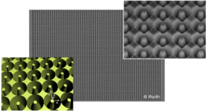
Figure 2: nano absorber structure in Gold with 400 nm outer diameter holes (design on the lower left, patterning result on the upper right, total array in the centre) – Zhejiang University (China)
Alternatively to Gallium the ionLINE Plus operates also with focused Gold or Silicon ion beams. For some applications contamination of the sample with Gallium is unwanted as it may change the physics of the device. Figure 3 shows an example of a plasmonic Gold structure on Silicon dioxide. This sample was patterned with a focused Silicon ion beam. In this case the milling is with a ?neutral? species ? Silicon making up the substrate ? and also with a less conductive species for better plasmonic results

Figure 3: Plasmonic Gold structure milled with a focused Silicon ion beam – University of Stuttgart (Germany)
Focused Gold and Silicon ion beams of the ionLINE Plus were also used for substrate functionalization by implantation, enabling e.g. the selective growth of Graphene nano ribbons on SiC substrates (S. Tongay et al, Drawing graphene nanoribbons on SiC by ion implantation, APPLIED PHYSICS LETTERS 100, 073501 (2012)). In particular Gold is a popular material for seeding and controlling subsequent growth processes.