
EVG?7300: NEW MULTI-FUNCTIONAL MICRO- / NANOIMPRINT AND LENS STACKING SOLUTION FROM EV GROUP FOR OPTICAL DEVICE MANUFACTURING
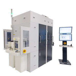
January 18, 2022 ? EV Group today introduced the EVG?7300 automated SmartNIL? nanoimprint and wafer-level optics system, the company?s most advanced solution to combine multiple UV-based process capabilities, such as nanoimprint lithography (NIL), lens molding and lens stacking (UV bonding), in a single platform. This industry-ready, multi-functional system is designed to serve advanced R&D and production needs for a wide range of emerging applications involving micro- and nano-patterning as well as functional layer stacking. These include wafer-level optics (WLO), optical sensors and projectors, automotive lighting, waveguides for augmented reality headsets, bio-medical devices, meta-lenses and meta-surfaces, and optoelectronics. Supporting wafer sizes up to 300 mm and featuring high-precision alignment, advanced process control and high throughput, the EVG7300 meets the HVM needs for a variety of freeform and high-precision nano- and micro-optical components and devices.
About EV Group
EV Group (EVG) is a leading supplier of equipment and process solutions for the manufacture of semiconductors, micromechanical systems (MEMS), compound semiconductors, power devices and nanotechnology devices. A recognized market and technology leader in wafer-level bonding and lithography for advanced packaging and nanotechnology, EVG?s key products include wafer bonding, thin-wafer processing and lithography/nanoimprint lithography (NIL) equipment, photoresist coaters, as well as cleaning and inspection/metrology systems. Founded in 1980, EVG services and supports an elaborate network of customers and partners all over the world. With more than 1100 employees worldwide, EVG is headquartered in Austria and operates fully-owned subsidiaries in the U.S., Japan, South Korea, China and Taiwan.
More information is available at www.EVGroup.com.