
Automation and throughput: Raith launches new Electron Beam Lithography tool
Given the size of a focused electron beam (on the order of one nano meter), electron beam lithography is an enabling technology for nano research. It is also used for the production of devices comprising nano-sized structures.
The company Raith is known as one of the leading suppliers of electron beam lithography tools. Well known sites like the renowned Graphene Centre in Manchester or the lab of IBM in Switzerland use the Raith EBPG Electron Beam Lithography systems for their research.
Raith is proud to announce its new family member, the EBPG5150, to the community.
This new electron beam lithography tool of the 100kV class is based on more than 45 years of experience in this field. With guaranteed sub 8nm resolution and the ability to write with ultra-high resolution in 1mm write fields it could be used to make large devices without stitching with the whole process run in a fully automated mode of operation. From the time of sample loading into the automatic airlock to the time the sample is removed no further manual intervention is required. The system is very efficient in its room layout being able to fit into less than 18square meter allowing easy access to all modules for service consideration.
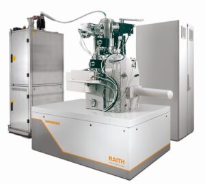
Picture 1 ?EBPG5150
EBPG electron beam lithography tools are installed in both advanced nano centres, Universities and at industrial production facilities world-wide.
A nice example of research use (from Yale University) is shown in picture 2. The device shown (with a CNOT gate in the centre) comprises ring resonators, superconducting nanowire single-photon detectors, couplers, nano-electromechanical phase shifters and other functions – introduced in six lithography steps, including four steps of electron beam lithography. Such photonic chips are used to study quantum computation with photons. On long run complex quantum computers may arise from such work.
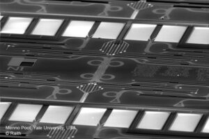
Picture 2 ? Raith micrograph award winning picture 2015 from Yale University
A well-known industrial application for the EBPG series is the make of high frequency electronics. At the heart of such devices are special T gate structures having a foot of possibly less than 20nm allowing them to operate in the range up to several 100 GHz. There is an endless list of applications for high frequency devices including test-&measurement, ultra-high speed communication (satellite communication) and radar. In this field EBPG tools provide the automation and throughput required to process thousands of wafers per year with high yield.
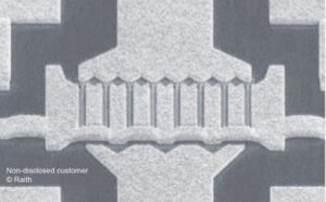
Picture 3: SEM micrograph of a multi-finger air bridge high frequency device (the vertical lines are the performance defining transistor gates)