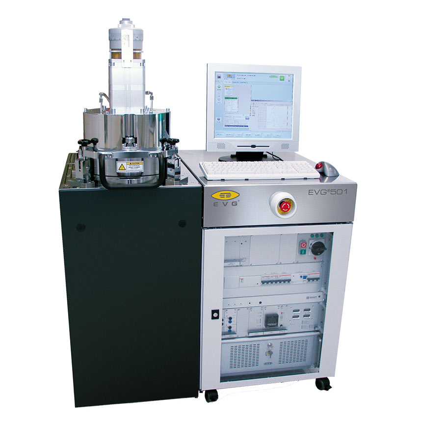
EVG501 Wafer bonding system
Description:
Versatile manual wafer bonding system for academia and industrial research
The EVG501 is a highly flexible wafer bonding system that can handle substrate sizes from single chips to 150 mm (200 mm in case of a 200 mm bond chamber). This tool supports all common wafer bonding processes such as anodic, glass frit, solder, eutectic, transient liquid phase, and direct. The easy access bond chamber and tooling design allows for quick and easy retooling for different wafer sizes and processes with a conversion time of less than 5 minutes. This versatility is ideal for universities, R&D facilities, or low-volume production. The design of the bond chambers is the same on the EVG high-volume-manufacturing tools, such as the EVG GEMINI, and the bonding recipes are easily transferable, allowing for easy scale up of production volumes.
Optimum total cost of ownership (TCO) for R&D and pilot line production
Real and low-force wafer wedge compensation system for highest yield
Unmatched pressure and temperature uniformity
Automated bond process execution and data logging
High-vacuum capable bond chamber (down to 10-5 mbar with turbo molecular pump)
Open chamber design for fast conversion and maintenance
Windows? based control software and operation interface
Smallest footprint for a 200 mm bonding system: 0.88 m2


